PN JUNCTION DIODE

Category –EE Online Test
Telegram-Join Us On Telegram
Attempt Free PN JUNCTION DIODE Here. Read The Important Electrical MCQ From Below.
l. The conventional current in a PN junction diode flows:
(a) From positive to negative
(b) From negative to positive
(c) In the direction opposite to the electron flow.
(d) Both (a) and (c) above
ANS-d
2. The cut in voltage (or knee voltage) of a silicon diode is
(a) 0.2V
(b) 0.6V
(c) 0.8 V
(d) l.0V
ANS-b
PN JUNCTION DIODE
3. When a diode is reverse biased, it is equivalent to
(a) An OFF switch
(b) an ON switch
(c) A high resistance
(d) none of the above
ANS-a
4. The resistance of a diode is equal to
(a) Ohmic resistance of the P- and N- semiconductors
(b) Junction resistance
(c) Reverse resistance
(d) Algebraic sum of (a) and (b) above
ANS-d
5. For a silicon diode, the value of the forward – bias voltage typically
(a) Must be greater than 0.3V
(b) Must be greater than 0.7V
(c) Depends on the width of the depletion region
(d) Depends on the concentration of majority carriers
ANS-b
PN JUNCTION DIODE
6. When forward biased, a diode
(a) Blocks current
(b) conducts current
(c) Has a high resistance
(d) drops a large voltage.
ANS-b
7. A PN junction diode’s dynamic conductance is directly proportional to
(a) The applied voltage
(b) the temperature
(c) The current
(d) the thermal voltage
ANS-c
PN JUNCTION DIODE
8. The forward region of a semiconductor diode characteristic curve is where diode appears as
(a) Constant current source
(b) a capacitor
(c) An OFF switch
(d) an ON switch
ANS-d
9. At room temperature of 25 °C, the barrier potential for silicon is 0.7 V. lts value at l25° C is
(a) 0.5V
(b) 0.3V
(c) 0.9V
(d) 0.7V
ANS-a
l0.Junction breakdown of a PN junction occurs
(a) With forward bias
(b) with reverse bias
(c) Because of manufacturing defect
(d) None of these
ANS-b
PN JUNCTION DIODE
11. Reverse saturation current in a silicon PN junction diode nearly doubles for every
(a) 2° C rise in temperature
(b) 5° C rise in temperature
(c) 6° C rise in temperature
(d) l0° C rise in temperature
ANS-d
l2.The approximate value of v0 across the diode shown in Fig below is

(a) Zero
(b) l0V
(c) 5V
(d) dependent on the value of R
ANS-a
PN JUNCTION DIODE
l3. The diode D is an ideal in the circuit shown in Fig below. The current, I will be
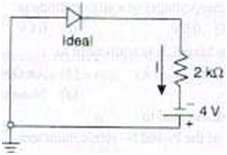
(a) – 2nA
(b) zero
(c) 2 mA
(d) 4mA
ANS-c
l4. The voltage at Vl and V2 of the arrangement shown in Fig below will be respectively
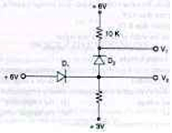
(a) 6V and 5.4V
(b) 5·4Vand 6V
(c) 3V and 5·4V
(d) 6V and 5V
ANS-d
PN JUNCTION DIODE
l5. The transition capacitance of a diode is l nF and it can withstand a reverse potential of 400V. A capacitance of 2nF which can withstand a reverse potential of l kV is obtained by connecting
(a) two l nF diodes in series
(b) six parallel branches with each branches comprising there l nF diodes in series
(c) two l nF diodes in series
(d) three parallel branches with each branch comprising lnF diodes in series
ANS-b
l6. A zener diode
(a) has a high forward-voltage rating
(b) has a sharp breakdown at low reverse voltage
(c) is useful as an amplifier
(d) has a negative resistance
ANS-b
l7. A 5 V reference is drawn from the circuit shown in Fig below if the zener diode current is of 5mA, then R will be
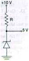
(a) 50fi
(b) 500 fi
(c) 5000 fi
(d) 50,000 fi
ANS-c