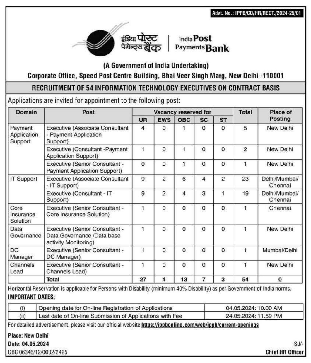
Electronics Devices And Circuits Part 7

Category –EE Online Test
Telegram-Join Us On Telegram
Attempt Free Electronics Devices And Circuits Part 7 Here. Read The Important Electrical MCQ From Below.
Answer
[2] A change in the value of the emitter resistance Re in a differential amplifier
Answer
[3] Generally, the gain of a transistor amplifier falls at high frequencies due to the
Answer
[4] In a common emitter, unbypassed resistor provides
Answer
Electronics Devices And Circuits Part 7
[5] A constant current signal across a parallel RLC circuits gives an o/p of 1.4V at the signal frequency of 3.89kHz. At the frequency of 4 kHz, the o/p voltage will be
Answer
[6] Class AB operation is often used in power (large signal) amplifiers in order to
Answer
[7] The bandwidth of an RF tuned amplifier is dependent on
Answer
[8]Most of the linear ICs are based on the two-transistor differential amplifier because of its
Answer
Electronics Devices And Circuits Part 7
[9] Negative feedback in an amplifier
Answer
10] A dc power supply has no-load voltage of 30V and a full-load voltage of 25V at full-load current of 1A. Its output resistance and load regulation respectively are
Answer
Electronics Devices And Circuits Part 7