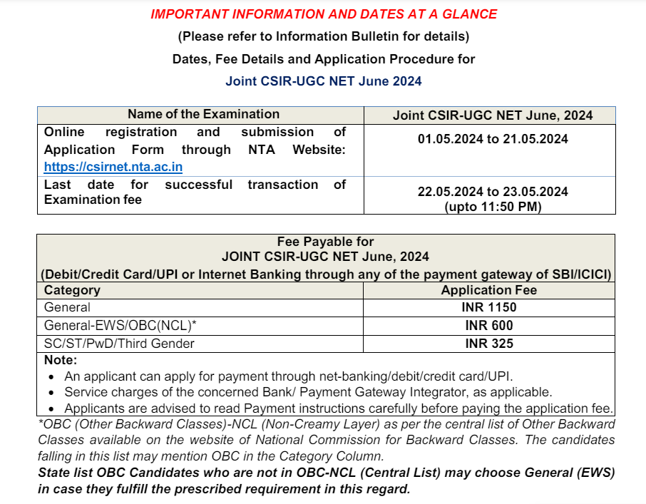
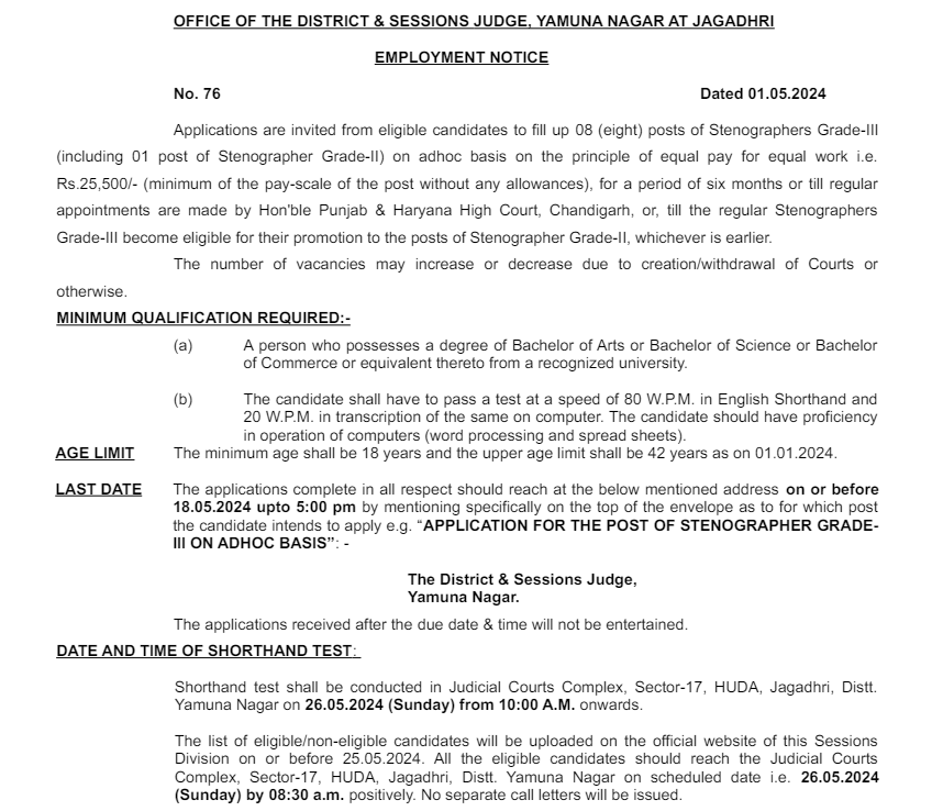
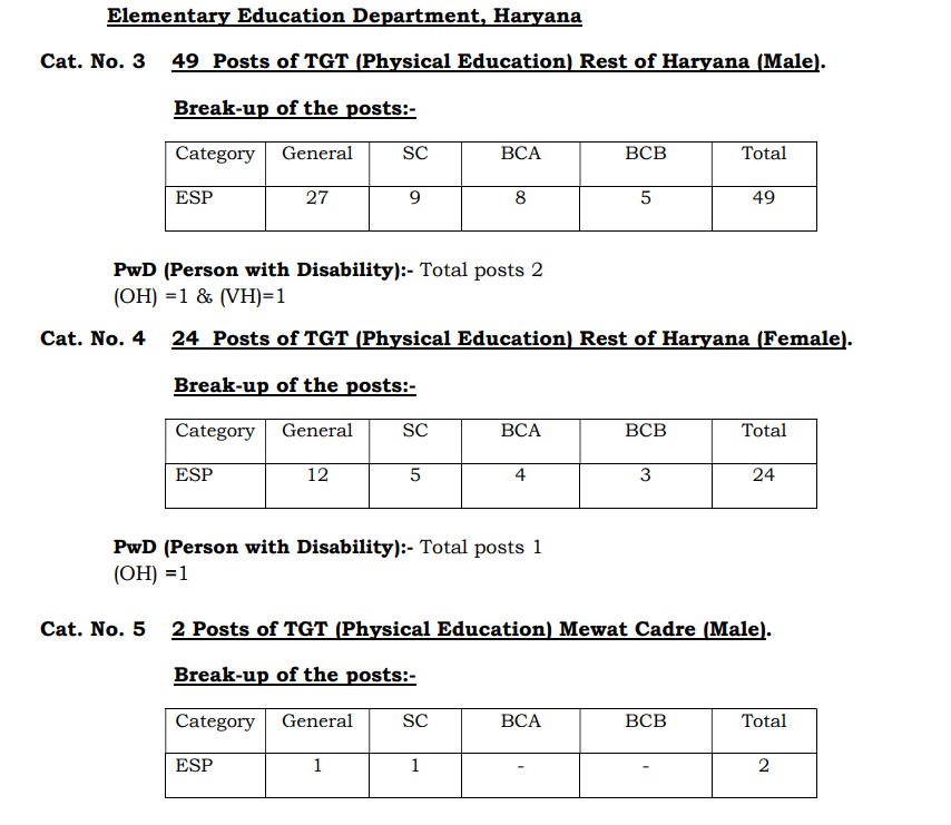
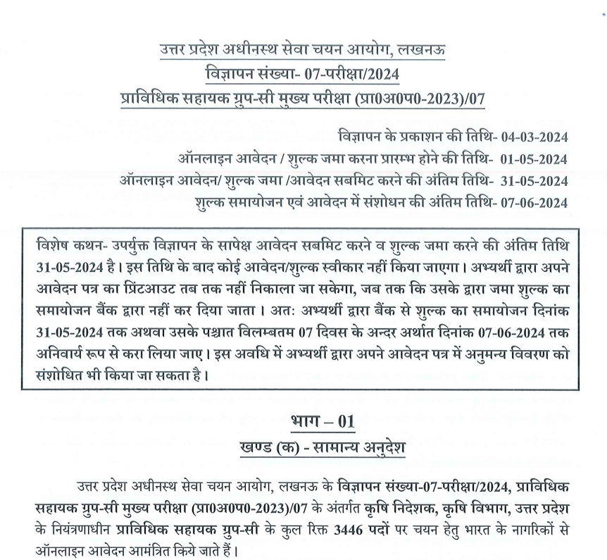
Electrical Analog Electronics Questions

Category –EE MCQ PDF
Telegram-Join Us On Telegram
Attempt Free Electrical Analog Electronics Questions Here. Read The Important Electrical Analog Electronics Questions MCQ From Below.
1. The early effect in a bipolar junction transistor is caused by
A. fast turn-on
B. fast turn-off
C. large collector-base reverse bias
D. large emitter-base forward bias
Answer: C
2. MOSFET can be used as a
A. current controlled capacitor
B. voltage controlled capacitor
C. current controlled inductor
D. voltage controlled inductors
Answer: B
3. Thermal runaway is not possible in FET because as the temperature of FET increases
A. the mobility decreases
B. the transconductance increases
C. the drain current increases
D. none of the above
Answer: A
4. A source follower using an FET usually has a voltage gain which is
A. greater than +100
B. slightly less than unity but positive
C. exactly unity but negative
D. about -10
Answer: A
5. A differential amplifier has a differential gain of 20,000 . CMRR=80 dB. The common mode gain is given by
A. 2
B. 1
C. 1/2
D. 0
Answer: A
Electrical Analog Electronics Questions
6. The approximate input impedance of the OPAMP circuit which has Ri=10k,Rf=100k,RL=10k
A. ∞
B.120k
C.110k
D.10k
Answer: D
7. An OPAMP has a slew rate of 5 V/µ S .The largest sine wave O/P voltage possible at a frequency of 1MHZ is
A. 10 volts
B. 5 volts C. 5/ volts
D.5/2 volts
Answer: D
8. A change in the value of the emitter resistance Re in a differential amplifier
A. affects the difference mode gain Ad
B. affects the common mode gain Ac
C. affects both Ad and Ac
D. does not effect either Ad and Ac
Answer: B
9. A differential amplifier is invariably used in the i/p stage of all OP-AMPs.This is dome basically to provide the OP-AMPs with a very high
A.CMRR
B. bandwidth
C. slew rate
D. open-loop gain
Answer: A
10. The effective channel length of a MOSFET in a saturation decreases with increase in
A. gate voltage
B. drain voltage
C. source voltage
D. body voltage
Answer: B
Electrical Analog Electronics Questions
11. Which of the following is not associated with a p-n junction
A. junction capacitance
B. charge storage capacitance
C. depletion capacitance
D. channel length modulation
Answer: D
12. In a p-n junction diode under reverse bias , the magnitude of electric field is maximum at
A. the edge of the depletion region on the p-side
B. the edge of the depletion region on the n-side
C. the p-n junction
D. the center of the depletion region on the n-side
Answer: C
13. An n- channel JFET has IDSS=2mA,and Vp=-4v.Its transconductance gm=in mA/V)for an applied gate to source voltage VGS=-2v is
A.0.25
B.0.5
C.0.75
D.1
Answer: B
14. In a common emitter, un by passed resister provides
A. voltage shunt feedback
B. current series feedback
C. negative voltage feedback
D. positive current feedback
Answer: C
15. A constant current signal across a parallel RLC circuits gives an o/p of 1.4v at the signa frequency of 3.89KHZ and 4.1KHZ .At the frequency of 4KHZ,the o/p voltage will be
A.1 v
B. 2v
C.1.4v
D.2.8v
Answer: B
Electrical Analog Electronics Questions
16. Class AB operation is often used in power large signal) amplifiers in order to
A. get maximum efficiency
B. remove even harmonics
C. overcome a crossover distortion
D. reducing collector dissipation
Answer: C
17. The bandwidth of an RF tuned amplifier is dependent on
A. Q –factor of the tuned o/p circuit
B. Q –factor of the tuned i/p circuit
C. Quiescent operating point
D. Q-factor of the o/p and i/p circuits as well as quiescent operating point
Answer: A
18. If =0.98 , Ico=6µA and Iβ=100µAfor a transistor, then the value of Ic will be
A.2.3mA
B.3.2mA
C.4.6 mA
D.5.2Ma
Answer: D
19.The MOSFET switch in its on-state may be considered equivalent to
A. resistor
B. inductor
C. capacitor
D. battery
Answer: C
20. Most of the linear ICs are based on the two-transistor differential amplifier because of its
A. input voltage dependent linear transfer characteristic
B. high voltage gain
C. high input resistance
D. high CMRR
Answer: D
Electrical Analog Electronics Questions
21. Negative feedback in an amplifier
A. Reduces gain
B. Increase frequency &phase distortion
C. Reduces bandwidth
D. Increases noise
Answer: A
22. A dc power supply has no-load voltage of 30v,and a full-load voltage of 25v at full-load current of 1A.Its output resistance & load regulation ,respectively are
A. 5 Ω & 20 %
B. 25 Ω & 20 %
C. 5 Ω & 16.7 %
D. 25 Ω & 16.7 %
Answer: B
23. The current gain of a bipolar transistor drops at high frequencies because of
A. Transistor capacitances
B. High current effects in the base
C. Parasitic inductive elements
D. The early effect
Answer: A
24. The ideal OP-AMP has the following characteristics.
A. Ri=∞ ,A=∞ ,R0=0
B. Ri=0 ,A=∞ ,R0=0
C. Ri=∞ ,A=∞ ,R0=∞
D. Ri=0 ,A=∞ ,R0=∞
Answer: A
Electrical Analog Electronics Questions
25. An npn BJT has gm=38mA/v, cµ =10¯14 F, cπ =10¯13F and DC current gain β0=90.For this
transistor fT & fβ are
A. fT =1.64 x 10⁸ Hz & fβ = 1.47 x 10¹⁰ Hz.
B. fT =1.47 x 10¹⁰ Hz & fβ = 1.64 x 10⁸ Hz
C. fT =1.33 x 10¹² Hz & fβ = 1.47 x 10¹⁰ Hz
D. fT =1.47 x 10¹⁰ Hz & fβ = 1.33 x 10¹² Hz
Answer: B
26. A 741-type OP-AMP has a gain-bandwidth product of 1MHz.A non-inverting amplifier
using this opamp & having a voltage gain of 20db will exhibit -3db bandwidth of
A. 50 KHz
B. 100KHz
C. 1000/17 KHz
D. 1000/7.07 KHz
Answer: B
27.An amplifier using an opamp with slew rate SR=1v/µsec has a gain of 40db.if this amplifier has to faithfully amplify sinusoidal signals from dc to 20 KHz without introducing any slew-rate induced distortion, then the input signal level must not exceed
A. 795mV
B. 395mV
C. 795 mV
D. 39.5mV
Answer: C
Electrical Analog Electronics Questions
28. In the differential voltage gain & the common mode voltage gain of a differential amplifier are 48db &2db respectively, then its common mode rejection ratio is
A.23dB
B.25dB
C. 46dB
D. 50dB
Answer: C
29. Generally, the gain of a transistor amplifier falls at high frequencies due to the
A. Internal Capacitance of the device
B. Coupling capacitor at the input
C. Skin effect
D. Coupling capacitor at the output
Answer: A
30. An amplifier without feedback has a voltage gain of 50,input resistance os 1 KΩ & Output resistance of 2.5KΩ.The input resistance of the current-shunt negative feedbac amplifier using the above amplifier with a feedbacik factor of 0.2 is
A. 1/11KΩ
B. 1/5KΩ
C. 5KΩ
D. 11KΩ
Answer: A
31. The action of JFET in its equivalent circuit can best be represented as a
A. Current controlled Current source
B. Current controlled voltage source
C. Voltage controlled voltage source
D. voltage controlled current source
Answer: D
32. Three identical amplifiers with each one having a voltage gain of 50,input resistance of 1KΩ& output resistance of 250 ,are cascaded. The open circuit voltage gain of combined amplifier is
A. 49dB
B. 51dB
C. 98dB
D. 102dB
Answer: C
Electrical Analog Electronics Questions
33. An ideal OP-AMP is an ideal
A. Current controlled Current source
B. Current controlled voltage source
C. Voltage controlled voltage source
D. voltage controlled current source
Answer: B
34. In a full-wave rectifier using two ideal diodes,Vdc & Vm are the dc & peak values of the voltage respectively across a resistive load. If PIV is the peak inverse voltage of the diode, then the appropriate relationships for this rectifier is.
A. Vdc = Vm/π, PIV=2Vm
B. Vdc = 2Vm/π, PIV=2vm
C. Vdc = 2Vm/π, PIV=Vm
D. Vdc = Vm/π, PIV=Vm
Answer: B
35. The cascade amplifier is a multistage configuration of
A. CC-CB .
B. CE-CB
C. CB-CC
D. CE-CC
Answer: B
36. The current gain of a BJT is
A. gm r0
B. gm / r0
C. gm rπ
D. gm /rπ
Answer: C
Electrical Analog Electronics Questions
37. The most commonly used amplifier in sample & hold circuits is
A. A unity gain non-inverting amplifier
B. A unity gain inverting amplifier
C. An inverting amplifier with a gain of 10
D. An inverting amplifiers with a gain of 100
Answer: B
38. To prevent a DC return between source and load, it is necessary to use
A. resistor between source and load
B. inductor between source and load
C. capacitor between source and load
D. either A. or B.
Answer: C
39. Introducing a resistor in the emitter of a common amplifier stabilizes the dc operating point
against variations in
A. Only the temperature
B. only the β of the transistor
C. Both Temperature & β
D. None of the above
Answer: C
40. Voltage Series feedback also called series-shunt feedback) results in
A. Increase in both input & output impedances
B. Decreases in both input & output impedances
C. Increase in input impedance & decreases in output impedance
D. Decrease in input impedance & increase in output impedance
Answer: C
41. The encapsulation of transistor is necessary for
A. preventing radio interference
B. preventing photo-emission effects
C. avoiding loss of free electrons
D. mechanical ruggedness
Answer: D
Electrical Analog Electronics Questions
42. In a transistor leakage current mainly depends on
A. doping of base
B. size of emitter
C. rating of transistor
D. temperature
Answer: D
43. In a CB amplifier the maximum efficiency could be
A. 99%
B. 85%
C. 50%
D. 25%
Answer: D
44. When a transistor is connected in common emitter mode, it with have
A. negligible input resistance and high output resistance
B. high input resistance and low output resistance
C. medium input resistance and high output resistance
D. low input resistance as well as output resistance
Answer: C
45. In all base driver amplifiers
A. ac collector voltage is 180° out of phase with ac base voltage
B. ac emitter voltage is 180° out of phase with ac base voltage
C. ac collector voltage is in phase with ac base voltage
D. none of the above
Answer: A
Electrical Analog Electronics Questions
46. The horizontal intercept of dc load line is the same as ideal
A. cut off point
B. saturation point
C. operating point
D. quasi saturation point
Answer: A
47. In deriving ac equivalent circuit for an amplifier circuit we short
circuit
A. all resistors
B. all transistors
C. all inductors
D. all capacitors
Answer: D
48. Which of the following statements is false?
A. Push pull signals are equal and opposite in phase
B. Class AB operation cannot be used for a push pull audio power output phase
C. A push pull output transformer has a centre-tapped primary
D. All of the above
Answer: B
49. Which of the following amplifier circuit using junction transistor has
the best gain?
A. Common base
B. Common emitter
C. Common collector
D. All have the same gain
Answer: B
50. In an op-amp differentiator
A. the amplitude of output is proportional to rate of change of input
B. the amplitude of output is proportional to input
C. output occurs when input is finite and constant
D. polarity of input and output is the same
Answer: A
Electrical Analog Electronics Questions