Electronics Radio Receiver Questions 2

Category –ECE MCQ PDF
Telegram-Join Us On Telegram
Attempt Free Electronics Radio Receiver Questions 2 Here. Read The Important Electronics Radio Receiver 2 MCQ From Below.
1)Among the bipolar logic families is specifically adopted for high speed applications?
a. Diode Transistor Logic (DTL)
b. Transistor Transistor Logic (TTL)
c. Emitter Coupled Logic (ECL)
d. Integrated Injection Logic (I2L)
ANSWER: Emitter Coupled Logic (ECL)
2) Which type of unipolar logic family exhibits its usability for the applications requiring low power consumption?
a. PMOS
b. NMOS
c. CMOS
d. All of the above
ANSWER: CMOS
3) Which type of output current flows towards or into the output terminal in a logic circuit?
a. Sourcing current
b. Sinking current
c. Both a and b
d. None of the above
ANSWER: Sinking current
4) Suppose that the digital IC family has a fan out of 6. It implies that the gate can supply the current to _______ of same family.
a. 6 inputs
b. 6 outputs
c. 12 nodes
d. 12 branches
ANSWER: 6 inputs
5) Which kind of logical operation is performed by the gate shown below?
 a. logical multiplication
b. Inversion
c. Addition/ Subtraction
d. NOT EXOR
ANSWER: Addition/ Subtraction
Electronics Radio Receiver Questions 2
6) What does the below stated OR Law imply, while performing OR operation of an input
with ‘1’? Expression of OR Law: A+ 1 = 1
a. output will always be equal to input
b. Output will always be high
c. Output will always be low
d. Output will always be same
ANSWER: Output will always be high
7) Which De Morgan’s theorem states that the complement of a sum is equal to the product of complements?
a. AB = A + B
b. A+B = A. B
c. A+B = A.B
d. AB = A + B
ANSWER: A+B = A. B
8) How is the relation specified between input and output in logic circuits?
a. Switching equations
b. Truth-table
c. Logic diagram
d. All of the above
ANSWER: All of the above
9) In the half subtractor combinational circuit, what does ‘A’ represent in the subtraction operation (A – B)?
a. Minuend bit
b. Maxend bit
c. Subtrahend bit
d. Suptrahend bit
ANSWER: Minuend bit
10) Which is an incorrect rule of binary subtraction from the following?
a. 0 – 0 = 0
b. 0 – 1 = -1
c. 1 – 0 = 1
d. 0 – 1 = 1 with borrow ‘1’
ANSWER: 0 – 1 = -1
11) What should be the output of converter, if a common anode display segment is to beturned ‘ON’?
a. ‘0’
b. ‘1’
c. Both a and b
d. None of the above
ANSWER: ‘0’
12) Which adder plays a crucial role in eliminating the problem associated with the inter-stage carry delay?
a. Half adder
b. full adder
c. BCD adder
d. Look-ahead carry adder
ANSWER: Look-ahead carry adder
13) Which among the following is/are responsible for the occurrence of clock skew by introducing delays from different paths of clock generator to various circuits?
a. Different length of wires
b. Gates on the paths
c. Gating of clock to control the loading of registers
d. All of the above
ANSWER: All of the above
Electronics Radio Receiver Questions 2
14) Consider the cross-coupled inverter shown below. By performing reset and set operations, if the circuit continue to remain in reset and set states respectively,then what is the bit storage capacity of cross-coupled inverter?

a. 0
b. 1
c. 2
d. 4
ANSWER: 1
15) Which is the prohibited state/ condition in S-R latch and needs to be avoided due to unpredictable nature of output?
a. S = R = 0
b. S = 0, R = 1
c. S = 1, R = 0
d. S = R = 1
ANSWER: S = R = 1
16) What would be the characteristic equation of SR latch corresponding to the K-map schematic shown below?

a. S + RQn
b. S + RQn
c. S + RQn
d. S + RQn
ANSWER: S + RQn
17) What does the data in parallel form of representation in registers, known as?
a. Temporal Code
b. Spectral Code
c. Special Code
d. Factorial Code
ANSWER: Special Code
18) Which type of triggering is shown by the D flip flops in buffer registers for the temporary storage of digital words?
a. Positive level triggering
b. Negative level triggering
c. Positive edge triggering
d. Negative edge triggering
ANSWER: Negative edge triggering
Electronics Radio Receiver Questions 2
19) Referring to the diagram, if all inputs are loaded simultaneously and output is loaded bit by bit, then what will be the mode of operation for a shift register?

a. Serial Input Serial Output (SISO)
b. Serial Input Parallel Output (SIPO)
c. Parallel Input Serial Output (PISO)
d. Parallel Input Parallel Output ( PIPO)
ANSWER: Parallel Input Serial Output (PISO)
20) When the mode control pin is connected to ground, Universal Shift Register acts as
_______
a. Unidirectional register
b. Bidirectional register
c. Multi-directional register
d. None of the above
ANSWER: Bidirectional register
21) The output of Up counters goes on increasing due to _________
a. Transmission of clock pulses
b. Reception of clock pulses
c. Both a and b
d. None of the above
ANSWER: Reception of clock pulses
22) If the number of states in a counter are 2n, then the value of ‘n’ is________
a. Less than the number of flip flops
b. Greater than the number of flip flops
c. Equal to the number of flip flops
d. Unpredictable
ANSWER: Equal to the number of flip flops
23) Which sequential circuits are applicable for counting pulses?
a. Counters
b. Flip Flops
c. Registers
d. Latches
ANSWER: Counters
24) Which type of triggering phenomenon is exhibited by Counters?
a. Edge
b. Level
c. Pulse
d. All of the above
ANSWER: Edge
Electronics Radio Receiver Questions 2
25) Where do/does the status of memory element in a synchronous sequential circuit get/s affected due to change in input?
a. At an active edge of clock
b. At passive edge of clock
c. Both a and b
d. None of the above
ANSWER: At an active edge of clock
26) Which type of memory elements are used in synchronous sequential circuits?
a. Clocked Flip flops
b. Unclocked Flip flops
c. Time Delay Elements
d. All of the above
ANSWER: Clocked Flip flops
27) According to Moore circuit, the output of synchronous sequential circuit depend/s on
______ of flip flop
a. Past state
b. Present state
c. Next state
d. External inputs
ANSWER: Present state
28) From the generalized schematic of Moore circuit given below, what does the combinational circuit ‘C1’ known as?

a. Previous state decoder
b. Present state decoder
c. Next state decoder
d. Output state decoder
ANSWER: Next state decoder
29) Which among the following are used in programming array logic (PAL) for reducing the loading on inputs?
a. Input buffers
b. Output buffers
c. OR matrix
d. AND matrix
ANSWER: Input buffers
30) If the number of nichrome fuse links in PAL are equal to 2M xn, then what does
‘n’ represent in it?
a. Number of inputs
b. Number of arrays
c. Number of outputs
d. Number of product terms
ANSWER: Number of product terms
31) Which gates are used on the output side as buffers in order to provide a
programmable output polarity in PAL 16 P8 devices?
a. AND
b. OR
c. EX-OR
d. NAND
ANSWER: EX-OR
Electronics Radio Receiver Questions 2
32) How many logic gates can be implemented in the circuit by complex programmable logic devices (CPLDs)?
a. 10
b. 100
c. 1000
d. 10000
ANSWER: 10000
33) Which bus is used as input data bus by the control lines for a specific duration while performing write operation?
a. Uni-directional bus
b. Bi-directional bus
c. Multi- directional
d. None of the above
ANSWER: Bi-directional bus
34) Which operations are executed by the control line at logic ‘1’ level?
a. Read
b. Write
c. Store
d. All of the above
ANSWER: Read
35) Which among the following is/are a/the major disadvantage/s of dynamic memory in
shift registers?
a. Less power consumption
b. High packaging density
c. Necessity of additional circuitry for time to time refreshing
d. All of the above
ANSWER: Necessity of additional circuitry for time to time
refreshing
36) Which among the following memories utilizes the electrical voltage for erasing purposes?
a. PROM
b. EAROM
c. RAM
d. CAM
ANSWER: EAROM
37) The ability of HDL to describe the performance specification of a circuit is regarded as ____
a. Test case
b. System case
c. Mark bench
d. Test bench
ANSWER: Test bench
38) What does an entity specify in the VHDL program format?
a. List of all libraries associated with the design
b. Code properties of VHDL
c. Input/output pins of the circuit
d. The behaviour of circuit
ANSWER: Input/output pins of the circuit
Electronics Radio Receiver Questions 2
39) Which among the following is the correct way of declaring the standard library in VHDL?
a. std. standard_ all
b. std _ standard .all
c. standard _ std. _all
d. std. standard .all
ANSWER: std. standard. all
40) Which mode in VHDL allows to make the signal assignments to a port of mode out by preventing it from reading?
a. In
b. Out
c. Inout
d. Buffer
Rank Math SEO
ANSWER: Inout
41) From where do the voltage noise get induced into the logic circuit?
a. From a gate output to load
b. From the connecting wires used between two gates
c. Both a and b
d. None of the above
ANSWER: Both a and b
42) If a high logic output drives a logic circuit input, which among the below specified reasons will be responsible in causing a voltage drop into an invalid state?
a. Positive noise spike greater than VNL
b. Positive noise spike less than VNL
c. Negative noise spike greater than VNH
d. Negative noise spike less than VNH
ANSWER: Negative noise spike greater than VNH
43) What is the standard percentage level used for measuring the propagation delay between the points corresponding to the inverter diagram shown below?

a. 20%
b. 50%
c. 70%
d. 100%
ANSWER: 50%
Electronics Radio Receiver Questions 2
44) What should be the value of input voltage for an efficient operation of a logic circuit by avoiding the conditions of invalid voltage levels?
a. Lower than VIL (max)
b. Higher than VIH (min)
c. Both a and b
d. None of the above
ANSWER: Both a and b
45) Which is the correct sequential order of operational steps executed in the
combinational logic circuits?
A. Operation of combinational gates over the inputs
B. Acceptance of n-different inputs
C. Generation of ‘m’ different outputs as per the required level
a. A, B, C
b. A, C, B
c. B, A, C
d. C, A, B
ANSWER: B, A, C
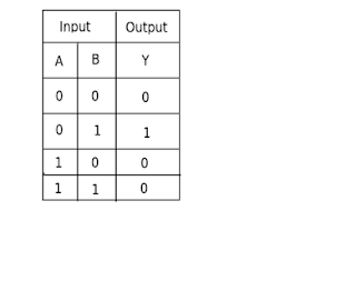
46) For the given truth-table, what is the logical expression in the standard SOP form?

a. Y = Σm (0,1)
b. Y = Σm (1,2)
c. Y = Σm (2,3)
d. Y = Σm (3,4)
ANSWER: Y = Σm (1,2)
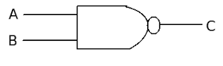
47) Which is the correct boolean expression for the logic circuit given below?

a. Y = (A.B) (A+ B) (A+C)
b. Y = (A.B) / (A + B) (A + C)
c. Y = (A.B) / (A + B) (A + C)
d. Y = (A.B)(A + B)(A+C)
ANSWER: Y = (A.B) (A+ B) (A+C)
48) Which code is used for labeling the cells of K-map?
a. Binary
b. Gray
c. BCD
d. ASCII
ANSWER: Gray
49) Which parameters are generated by the ripple carry propagation in the addition process of parallel adder?A. Propagation delay
B. Time delay
C. Carry delay
D. Speed delay
a. A & B
b. B & C
c. A & C
d. C & D
ANSWER: A & B
50) Which number/ code is added to an incorrect result obtained in BCD addition for correction purpose?
a. One (0001)
b. Three (0011)
c. Six (0110)
d. Nine (1001)
ANSWER: Six (0110)
Electronics Radio Receiver Questions 2
51) According to the truth-table given below, the output case for one-bit comparator is __________
a. A < B
b. A > B
c. A = B
d. None of the above
ANSWER: A < B
52) How many arithmetic operations can be performed by Arithmetic Logic Unit?
a. 10
b. 12
c. 16
d. 32
53) For the schematic shown below, if the rectangular signal is applied in the form of clock signal to edge-triggered flip-flop, then where will be the change in its output?

a. Only at rising edge
b. Only at falling edge
c. Either at rising edge or falling edge
d. Neither at rising edge nor at falling edge
ANSWER: Either at rising edge or falling edge
54) In delay flip-flop, _______ after the propagation delay.
a. Input follows input
b. Input follows output
c. Output follows input
d. Output follows output
ANSWER: Output follows input
55) Which among the following statements is correct for the triggering associated
a. Latch is level-triggered flip-flop
b. Latch is edge-triggered flip-flop
c. Flip-flop is edge-triggered latch
d. Flip-flop is not edge sensitive
ANSWER: Latch is level-triggered flip-flop
Electronics Radio Receiver Questions 2
56) T flip- flop finds its application in the form of frequency division since it divides the clock frequency by ________
a. 2
b. 4
c. 2n – 1
d. 4n – 1
ANSWER: 2
57) Which is the correct sequence of operations to be necessarily performed in the resistance welding application of ring counter?
a. Hold, Squeeze, Weld, Off
b. Squeeze, Hold, Weld, Off
c. Weld, Squeeze, Hold, Off
d. Off, Squeeze, Hold, Weld
ANSWER: Squeeze, Hold, Weld, Off
58) For a ring counter, the number of output states are always equal to ______
a. Number of input states
b. Number of clock pulses
c. Number of registers
d. Number of flip flops
ANSWER: Number of flip flops
59) On the second falling edge of clock in ring counter, if the generated output of second clock pulse is ‘ 0100’, what will be the output after the fourth clock pulse?
a. 1000
b. 0001
c. 0010
d. 0000
ANSWER: 0001
60) If a complete sequence is detected, what will be the output of a sequence detector?

a. 1
b. 0
c. Both a and b
d. None of the above
ANSWER: 1
61) If the output of two-bit asynchronous binary up counter using T flip flops is ’00’ at reset condition, then what output will be generated after the fourth negative clock edge?
a. 00
b. 01
c. 10
d. 11
ANSWER: 00
Electronics Radio Receiver Questions 2
62) On which factor/s does the clock pulse frequency of a counter depend/s for its reliable operation?
a. Number of flip flops
b. Width of strobe pulse
c. Propagation delay
d. All of the above
ANSWER: All of the above
63) Which flip flops serve to be the fundamental building blocks of counters?
a. R flip flops
b. J-K flip flops
c. T flip flops
d. D flip flops
ANSWER: T flip flops
64) Why is the extent of propagation delay in synchronous counter much lesser than that of asynchronous counter?
a. Due to clocking of all flip flops at the same instant
b. Due to increase in number of states
c. Due to absence of connection between output of preceding flip flop and clock of next one
d. Due to absence of mode control operation
ANSWER: Due to clocking of all flip flops at the same instant
65) Where are signals received from, at the output decoder in generalized form of Mealy circuit?
A. Input of memory elements
B. Output of memory elements
C. External inputs
D. External outputs
a. A & D
b. B & C
c. B & D
d. A & C
ANSWER: B & C
66) Consider the state equation given below. If R.H.S of an equation is zero, then what would be the value of L.H.S (next state) after the application of a clock pulse? QA(n + 1) = (QA QB + QA QB) x + QA QB
a. zero
b. Infinity
c. QA QB x
d. QA QB x
ANSWER: Zero
67) Which among the following state machine notations are generated outside the sequential circuits?
a. Input variables
b. Output variables
c. State variables
d. Excitation variables
ANSWER: Input variables
68) Which mechanism allocates the binary value to the states in order to reduce the cost of the combinational circuits?
a. State Reduction
b. State Minimization
c. State Assignment
d. State Evaluation
ANSWER: State Assignment
Electronics Radio Receiver Questions 2
69) Which type of CPLD packaging can provide maximum number of pins on the package due to small size of the pins?
a.PLCC
b. QFP
c. PGA
d. BGA
ANSWER: BGA
70) What is/are the configurable functions of each and every IOBs connected around the FPGA device from the operational point of view?
a. Input operation
b. Tristate output operation
c. Bi-directional I/O pin access
d. All of the above
ANSWER: All of the above
71) What would happen, if smaller logic modules are utilized for performing logical functions associated with FPGA?A. Propagation delay will increase
B. FPGA area will increase
C. Wastage of logic modules will not be prevented
D. Number of interconnected paths in device will decrease
a. A & B
b. C & D
c. A & D
d. B & C
ANSWER: A & B
72) In JTAG programming, JTAG stands for ________
a. Joint Texture Analysis Group
b. Joint Technique Aided Group
c. Joint Testing Array Group
d. Joint Test Action Group
73) Which operations are likely to get performed by the Content Accessible Memories (CAM) in addition to read/write operations executed by conventional ?
a. Association
b. Distribution
c. Commutation
d. Identification
ANSWER: Association
74) Which among the following techniques is used by EPROM for erasing purpose?
a. Force Convection
b. Ultraviolet Radiation
c. Photo-conduction
d. None of the above
ANSWER: Ultraviolet Radiation
Electronics Radio Receiver Questions 2
75) Which among the following specifies the minimum amount of time necessary for data validation after the termination of the write pulse?
a. Write pulse time
b. Write release time
c. Data set up time
d. Data hold up time
ANSWER: Data hold up time
76) Which parameter of read cycle timing characteristics defines the maximum time delay between the beginning of read pulse and output buffers arriving at active state from Hi-z condition?
a. Read to output valid time
b. Read to output active time
c. Access time
d. Output tristate from read time
ANSWER: Read to output active time
77) Which among the following is the correct way of entity representation for the
two input NAND gate shown below?
a. NAND 5 entity is port (A, B : input; C: output); NAND 5 end;
b. entity NAND5 is port (A, B : in bit; C: out bit); end NAND 5;
c. Entity: NAND5 port(Inputs: A, B; Output : C);end;
d. entity : NAND5 port( inbit : A,B), ( outbit: C); end.
ANSWER: entity NAND5 is port (A, B : in bit;C: out bit);end NAND 5;
78) Which type of architectural modeling style describes the internal design details in the form of a set representing the interconnected components?
a. Dataflow
b. Behavioral
c. Structural
d. Mixed
ANSWER: Structural
Electronics Radio Receiver Questions 2
79) Dataflow style of architectural modeling is represented as a set of ___________ assignment statements.
a. Sequential
b. Concurrent
c. Random
d. Combinational
ANSWER: Concurrent
80) How are the design specifications represented in the behavioral modeling style of VHDL?
a Boolean equation
b. Truth table
c. Logical diagram
d. State diagram
ANSWER: Truth table
81) If power dissipation and propagation delay in a logic circuit areestimated to be 55mW and 20ns respectively, what will be its figureof merit?
a. 1.10 nanojoule
b. 1.65 nanojoule
c. 2.50 nanojoule
d. 5.5 nanojoule
ANSWER: 1.10 nanojoule
82) What does the diode D3 represents in the equivalent circuit of Multiple Emitter Transistor shown below?

a. Base to emitter junction
b. Collector to base junction
c. Collector to emitter junction
d. Emitter to emitter junction
ANSWER: Collector to base junction
83) Which is the correct order of sequence for representing the input values in
K-map?
a. (00, 01, 10, 11)
b. (00, 10, 01, 11)
c. (00, 01, 11, 10)
d. (00, 10, 11, 01)
ANSWER: (00, 01, 11, 10)
84) Which is the simplified equation of output for K-map consisting of four adjacent ones, given below?

a. A B
b. BD
c. CD
d. ABD
ANSWER: CD
85) Which type of combinational logic circuit is shown below?

a. Multiplexer
b. Demultiplexer
c. Encoder
d. Comparator
ANSWER: Multiplexer
86) Which among the following is an octal to binary priority encoder?
a. 74147
b. 74148
c. 74149
d. 74150
ANSWER: 74148
87) Which flip-flop plays a vital role by functioning as the basic building block of a ripple counter?
a. S-R flip-flop
b. J-K flip-flop
c. D flip-flop
d. T flip-flop
ANSWER: T flip-flop
88) Which among the following is not a mode of Flip Flop representation?
a. Characteristic Equations
b. Excitation Tables
c. Finite State Machines (FSM)
d. Variable Entered Mapping (VEM)
ANSWER: Variable Entered Mapping (VEM)
Electronics Radio Receiver Questions 2
89) In a sequence detector, if the required bit is at its input while checking the sequence bit by bit, the detector moves to ________
a. Previous state
b. Next state
c. Remains in the same state (present state)
d. Null state
ANSWER: Next state
90) Which among the following sequential logic circuits are adopted for the designing of a sequence generator?
a. Shift Registers
b. Counters
c. Both a and b
d. None of the above
ANSWER: Both a and b
91) From the diagram shown below, if the circuit enters into state ‘5’, its next state will be ‘7’. If the circuit further enters at state’7′, then what would be the desirable next state for avoiding the lock out condition?
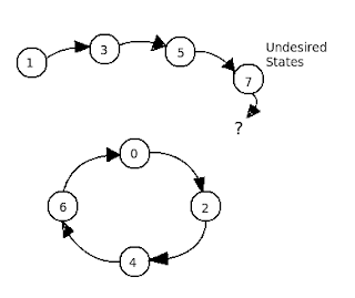
a. 0
b. 3
c. 5
d. 7
ANSWER: 0
92) Which among the following are the sequential circuits entering into the phenomenon of lock out condition?
a. Bush circuits
b. Bushless circuits
c. Locked circuits
d. Unlocked circuits
ANSWER: Bushless circuits
93) How many ‘D’ flip flops will be required for designing the synchronous counter for the state diagram shown below?

a. 2
b. 3
c. 5
d. 7
ANSWER: 3
94) The mechanism of ‘Bushing’ specifically refers to the addition of __________ in the state diagram
a. Nodes
b. Branches
c. Loops
d. States
ANSWER: Branches
95) From the K-map given below, what would be the state equation of D Flip Flop?

a. Qn+1 = QnD
b. Qn+1 = QnD
c. Qn+1 = D
d. Qn+1 = D
ANSWER: Qn+1 = D
96) In the below drawn schematic, what does an arrow between the circles indicate?

a. Present state
b. Next state
c. State transition
d. Don’t care condition
ANSWER: State transition
97) Which among the following statement/s is/are not an/the advantage/s of Programmable Logic Devices (PLDs)?
a. short design cycle
b. Increased space requirement
c. Increased switching speed
d. All of the above
ANSWER: Increased space requirement
Electronics Radio Receiver Questions 2
98) What do the Programmable Logic Devices (PLDs) designed specially for the combinational circuits comprise?
a. Only gates
b. Only flip flops
c. Both a and b
d. None of the above
ANSWER: Only gates
99) With the availability of 16 x 4 memory size, how many ICs ( memory chips) will be required for the expansion of its word size in order to obtain 16 x 8 memory?
a. 2
b. 4
c. 8
d. 16
ANSWER: 2
100) What is the bit storage capacity of TTL RAM cell?
a. 0
b. 1
c. 4
d. 16
ANSWER: 1
101) Which components play a significant role in the formation of a dynamic RAM?
a. Two MOSFETs
b. Two capacitors
c. One MOSFET and one capacitor
d. One MOSFET and two capacitors
ANSWER: One MOSFET and one capacitor
102) Which signal is used to transfer the stored data into RAM?
a. Store
b. Load
c. Recall
d. Move
ANSWER: Recall
103) Which among the following ROMs exhibit/s the necessity of eliminating the PROM from the circuit?
a. EPROM
b. EEPROM
c. Both a and b
d. None of the above
ANSWER: EPROM
Electronics Radio Receiver Questions 2
104) Which among the following does not belong to the category of sequential statements?
a. If statements
b. Process statements
c. Loop statements
d. Node statements
ANSWER: Node statements
105) Which type of logic is produced by case statements?
a. Serial logic
b. Parallel logic
c. Priority encoded logic
d. Priority decoded logic
ANSWER: Parallel logic
106) Which among the following is not a type of concurrent statement?
a. Simple signal assignment
b. Selected signal assignment
c. Generate statement
d. Direct Instantiation
ANSWER: Direct Instantiation
107) Match the following value kind attributes with their return elements :A. Value Type attribute ——————– 1) Length
B. Value Array attribute ——————- 2) Information
C. Value Block attribute ——————- 3) Bounds
a. A- 3, B- 1, C- 2
b. A- 1, B- 2, C- 3
c. A- 2, B- 1, C- 3
d. A- 2, B- 3, C-1
ANSWER: A- 3, B- 1, C- 2
Electronics Radio Receiver Questions 2